ISSN : 0976-8505
Der Chemica Sinica
Optical Characteristics of Manganous Doped Cadmium Oxide Thin Films Deposited by Spray Pyrolysis Method
1Department of Physics, K. Ramakrishnan College of Engineering, Tiruchirappalli, India
2Department of Physics, Urumu Dhanalakshmi College, Tiruchirappalli, India
3Department of Mechanical Engineering, K. Ramakrishnan College of Engineering, Tiruchirappalli, India
Abstract
The properties of cadmium oxide films are very similar to those of Mn doped CdO films. They are high resistance to mechanical and chemical degradation. In this article Mn doped CdO films have been deposited on the glass substrate and this optical characteristics are analyzed by using the spectrophotometer. Films are deposited on glass substrate at various temperatures ranged from 400°C-600°C by spray pyrolysis method.
Keywords:
CdO, Mn, Spray pyrolysis, Glass substrate.
Introduction
Oxides of many metals such as Tin, Indium, Zinc, Cadmium and their alloys, can be used as TCO’s possessing transparent conducting property. Most of the studied transparent conducting metal oxides are anion deficient (i.e., Oxygen deficient) and hence are always n-type conductors [1]. These films can exhibit various characteristics of metals, semiconductors and insulators with improved electrical and optical properties. So they can be used as electrodes in optoelectronic devices [2], display devices [3] and photovoltaic cells [4]. CdO films can be synthesized by various methods such as Spray Pyrolysis [5], Sputtering [6], Sol-gel spin coating [7], Activated reactive evaporation [8], Metal Organic Chemical Vapour deposition (MOCVD) [9]. The transparent conducting metal CdO is coming under n-type semiconductor with 2.3 eV to 2.5 eV in direct band gap and 1.3 eV to 1.98 eV in indirect band gap [10-12]. This CdO doped films have the non-linear optical properties [13]. There has been a lot of work on the growth and physical properties of transparent conducting oxides which has lot of increasing applications [14]. These CdO doped films are common materials for detectors, gas sensors, and photovoltaic solar cells. Mn doped CdO films by spray pyrolysis technique and investigated the effect of Mn on electrical, optical, structural and surface properties of CdO films showed that it can be used in optoelectronic applications [15]. The Mn-doped CdO nano particles having the ferromagnetic behaviour at low concentration [16].
Experimental
Materials and methods
Solution of Cadmium acetate (0.2 M), Manganous chloride (0.1 M) are prepared by dissolving in distilled water. The ratio of Cadmium acetate and Manganous chloride is 2:1. Initially the glass substrate is heated around 450°C. After that the prepared solution was sprayed on the substrate. Then the substrate is slowly cooled. The experimental setup consists of an indigenously designed glass spray gun. It has two inlets. One is connected to a compressed air reservoir and the other is connected to the solution reservoir. The diameter of the spray gun is 0.0425 cm. The pressure of the air is measured by a pressure gauge. The deposit layers must be adherent to the substrates and there should not peel off from the substrates under the normal conditions of stress and strain, mechanical or thermal to which the deposits are exposed during their uses. A poor adhesion of a deposit to a substrate is primarily caused by the presence of a physical barrier between the deposit and the substrate at the interface due to oil, grease, undesired surface layers over the substrate surface. Presence of point defects, lattice misfits, grain misfits are also affect the deposition of film over the substrate. The effect of these can be often being reduced or completely eliminated by appropriate annealing at a suitable temperature or sometimes by varying the deposition conditions.
Results and Discussion
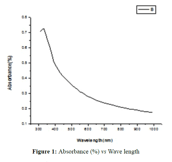
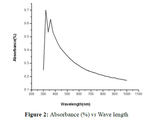
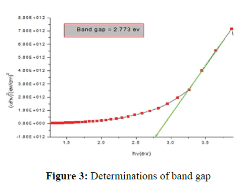
The thickness of the coated film was calculated by microbalance technique by using the formula t=w/Aρ. Where ‘w’ is weight difference of the film, ‘ρ’ is density and ‘A’ is deposition area. The thickness of Manganous doped CdO thin film is found to be 2.5 μm. The thickness of the thin film may varied by spraying time. The absorbance vs wavelength have been plotted for deposited thin film. From this graph the absorption co-efficient ‘a’ can be calculated for various values of wavelength. Figure 1 shows the absorption spectra of CdO. The absorption of CdO films was studied in the wavelength range 300-1000 nm. The optical absorbance of the films decreases with the wavelength. These spectra reveal that as-grown CdO films have more absorbance in the UV region and less absorbance in the visible and high wavelength region. In Figure 2 it is noted that the absorbance of CdO film varies between 300 to 400 nm, after that it will goes on degreasing. The band gap energy of the film on glass is determined by drawing the graph between hγ vs (αhγ)3/2 and it is indicated in Figure 3. The corresponding band energy gap was found to be 2.773 eV. This band gap may be changed due to the difference in the deposition method and the parameters used during the process of coating.
Conclusion
The Manganous doped CdO thin film was grown on glass substrate by spray pyrolysis method. The thickness of the doped film was calculated and it is found to be 2.5 μm. The absorption co-efficient ‘a’ can be calculated for various values of wavelength range 300- 1000 nm. This shows the optical absorbance of the films decreases with the wavelength. These spectra reveal that as-grown CdO films have more absorbance in the UV region and less absorbance in the visible and high wavelength region. The corresponding band energy gap was found to be 2.773 eV. This band gap may be changed due to the difference in the deposition method and the parameters used during the process of coating.
References
- Andreas Stadler (2012), Transparent Conducting Oxides—An Up-To-Date Overview, Materials 5:661-683.
- Radi PA,Brito-Madurro AG, Madurro JM, DantasBraz NO (2006), Characterization and properties of CdO nanocrystals incorporated in polyacrylamide, Braz. J. Phys 36:412-41.
- Yang Y, Qinglan H, Andrew WM, Shu J, Jun Ni et al (2005).Highly transparent and conductive CdO thin films as anodes for organic light-emitting diodes, Film micro structure and morphology effects on performance, J Soc Inf Display 9: 383-387.
- Raid AI,Omar AA (2007), A new route for fabricating CdO/c-Si heterojunction, Sol. Energy Mater Sol. Cells, 91: 903-907.
- Dong Ju Seo (2004), Structural and Optical Properties of CdO Films Deposited by Spray Pyrolysis, JKPS 45:1575-1579.
- Subramanyam TK, Uthanna S, Srinivasulu NB (1998), Preparation and characterization of CdO films deposited by dc magnetron reactive sputtering, Mater. Lett. 35: 214-220.
- Carballeda GDM, Castanedo PR, Jiménez SO, Jiménez S, Torres- DG et al.(2000), High transmittance CdO thin films obtained by the sol-gel method,Thin Solid Films 371: 105-108.
- Sravani IC, Ramakrishna RKT, Jayarama RP (1991), Physical behaviour of CdO films prepared by activated reactive evaporation, Semicond. Sci. Technol. 6: 1036-1038.
- Ellis DM, Irvine SJC (2004), MOCVD of highly conductive CdO thin films, J. Mater. Sci. Mater. Electron 15: 369-372.
- Peng XS, Wang XF, Wang YW, wang CZ, Meng GW et al. (2002),Novel method synthesis of Cdo nanowires,J.phys.D:Appl.phys. 35: L101-L104.
- Gurumurugan K, Mangalraj D, Narayandass SK, sekar K, Girija VCP (1994), Characterization of transparent conducting CdO films deposited by spray pyrolysis, Semicond.Sci. Technol. 9:1827-1832.
- Wu X, Wang R, Wang L, Liu S, Xu J et al(1998),Optical properties of nanometer sized CdO,organosol, J. Mater. Res.13:604-609.
- Gulino A, Compagnini G, Scalisi AA (2013), Large third-order nonlinear optical properties of cadmium oxide thin films, chem. Mater.15:3332-3336.
- Gal D, Hodes G, Lincot D, Schock HW (2000),Electrochemical deposition of zinc oxide films from non-aqueous solution: A new buffer /window process for thin film solar cells, Thin solid Films.361:79-83.
- Biasi De RS, Grillo MLN (2009), influence of manganese concentration on the electron magnrtic resonance spectrum of Mn2+in Cdo, Journal of Alloys and Compounds485: 26-28.
- Rajkumar N, Susila VM, Ramachandran K (2011), On the possibility of ferromagnetism in CdO: Mn at room temperature. J. Exp. Nanosci. 6:389-398.

Open Access Journals
- Aquaculture & Veterinary Science
- Chemistry & Chemical Sciences
- Clinical Sciences
- Engineering
- General Science
- Genetics & Molecular Biology
- Health Care & Nursing
- Immunology & Microbiology
- Materials Science
- Mathematics & Physics
- Medical Sciences
- Neurology & Psychiatry
- Oncology & Cancer Science
- Pharmaceutical Sciences


